Discover our top-performing medical-grade skincare systems customized for luxury beauty hubs in Shibuya, Ginza, and international consumer markets.
Tokyo is widely recognized as a global capital of cosmetic innovation and aesthetic engineering. The domestic Japanese home beauty device market is defined by a deep convergence between consumer electronics manufacturing giants and traditional cosmetic houses. Under Japan's rigorous Pharmaceutical and Medical Devices Act (PMDA) and electrical appliance regulations (PSE), the safety, design, and consistency profiles expected of Japanese products are exceptionally high.
Historically, the engineering behind domestic devices was driven by local microcurrent and radiofrequency (RF) research clusters. Today, as international demand for high-performance home skincare solutions surges, global beauty brands increasingly seek out production frameworks that merge Tokyo's design philosophies, materials selection, and quality management protocols with scalable, high-efficiency manufacturing capabilities.
To address this structural demand, Chengdu Osity Beauty Co., Ltd. has constructed a strategic, globally-integrated pipeline. By pairing Tokyo-inspired aesthetic configurations, precise optical layouts, and strict regulatory safety frameworks with Chengdu's advanced and cost-effective manufacturing infrastructure, we deliver high-performance private-label and customized skin tools. This model guarantees that brands receive devices with J-Beauty precision, medical-grade standards, and commercially competitive pricing models.
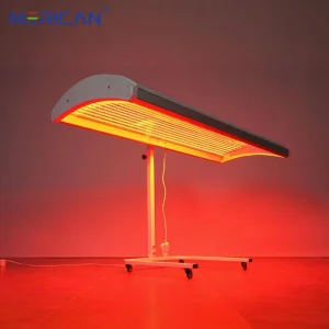
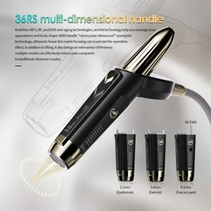
The global market for beauty devices is undergoing a structural transition. Consumers are moving away from superficial topicals toward physics-driven energy therapies—principally Photobiomodulation (PBM) via LED, High-Intensity Focused Ultrasound (HIFU), multi-polar Radiofrequency (RF) dermal heating, and localized Electrical Muscle Stimulation (EMS). Tokyo remains a core center for component sourcing, particularly for high-stability laser diodes and precision-engineered sensors.
Utilizing Japanese high-frequency chips for thermal monitoring and stable energy output, preventing epidermal burns while optimizing deep dermal remodeling.
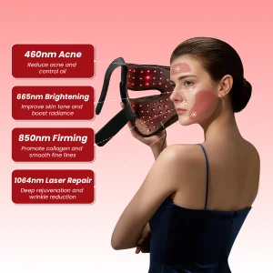
Exact nanometer wavelength outputs (633nm, 660nm, 850nm, 940nm, 1064nm) validated through high-precision optical spectrum analyzers.
Use of food-grade, high-elasticity silicones and surgical steel contact points to prevent allergic contact dermatitis under intense light or microcurrent cycles.
For international beauty brands and distributors, sourcing devices directly from traditional Japanese factories can present structural barriers, including elevated unit costs, long tooling lead times, and communication frictions. Chengdu Osity Beauty Co., Ltd. resolves these bottlenecks. By serving as an agile engineering and manufacturing partner, we translate Tokyo’s aesthetic standards, ergonomics, and material qualities into scalable, high-volume production lines. This allows partners to bring advanced beauty devices to market rapidly without sacrificing reliability or regulatory standards.
We do not simply manufacture; we engineer end-to-end device strategies. Chengdu Osity Beauty Co., Ltd. provides robust industrial solutions structured to minimize market friction and accelerate product rollouts for our global partners:
The home beauty industry is shifting toward highly personalized, data-integrated regimes. Below is the technical progression path our production team is targeting to support future-proof client portfolios:
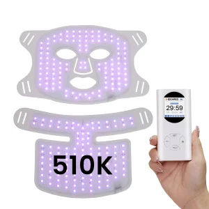
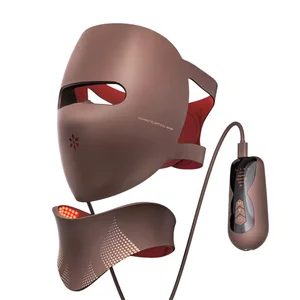
Embedding high-density, narrow-spectrum LEDs and 1064nm Near-Infrared lasers directly into flexible, medical-grade silicone mask architectures to maximize skin coverage and absorption.
Integrating low-energy Bluetooth (BLE) modules connecting devices to proprietary mobile apps. Real-time optical skin analysis adjusts device pulse frequency and duration dynamically based on localized moisture and pigmentation levels.
Replacing high-impact ABS plastics with plant-derived, compostable polymers that retain structural strength and electrical insulation properties, aligning with international carbon-neutral mandates.
Entering international beauty device markets requires navigating complex, regionally specific medical and consumer electronic standards. A single regulatory failure can result in port rejection, product seizures, or brand damage. We maintain an in-house compliance division to guide your products through global certifications:
We verify adherence to Japan's PSE (Electrical Appliance and Material Safety Act) requirements. Devices are designed with thermal-cutoff fuses, reliable double-insulated wiring, and electromagnetic interference shielding to pass METI inspections and gain immediate retail access in Tokyo, Osaka, and regional hubs.
For North American and European expansion, we manufacture in alignment with FDA (Class II Clearance pathways), CE-MDR (Medical Device Regulation), FCC, and RoHS directives. All circuit assemblies utilize lead-free components, and optical emission levels are verified to ensure eye-safety parameters conform to EN 62471.
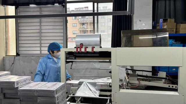
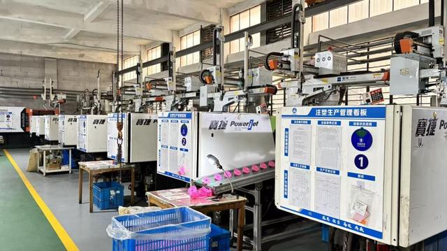
Our production facility operates under a rigorous ISO 13485 (Medical Devices Quality Management System) framework. Every single device undergoes a multi-stage testing loop before final packaging: structural load testing, high-voltage insulation tests, LED luminous flux verification, and waterproof chamber trials. This guarantees a defect rate below 0.1%, protecting your brand reputation and minimizing returns.
Addressing crucial technical and commercial questions from procurement directors, brand owners, and product developers seeking beauty device manufacturing solutions.
All RF tools feature integrated NTC thermistors that continuously read epidermal temperatures at 100 samples per second. If the surface temperature exceeds 42°C, the power output automatically throttles to prevent skin damage. Our LED devices utilize precise constant-current driver circuits to maintain stable luminous exitance, preventing flickering or light spikes.
The timeline spans industrial design and engineering blueprints (2–3 weeks), rapid 3D prototyping (1 week), mold fabrication and validation (4–6 weeks), followed by trial production and regulatory certification testing. Mass assembly typically takes 30-45 days post-sample sign-off, depending on component availability and batch scale.
This structure provides the optimal balance of engineering precision and cost-efficiency. Clients benefit from advanced optoelectronic and mechanical designs modeled on Tokyo's J-Beauty market standards, combined with the scalable manufacturing infrastructure, robust assembly pipelines, and cost advantages of Chengdu's technology parks.
Yes. We utilize food-grade and platinum-cured biocompatible silicones that comply with FDA and LFGB requirements. These materials are non-cytotoxic, sweat-resistant, and do not degrade, discolor, or leach compounds under prolonged exposure to sebum or cosmetics.
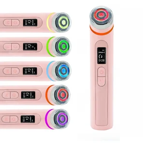
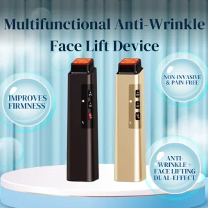
We offer comprehensive customization, including custom housing molds, tailored LED wavelength configurations (such as targeting specific acne-fighting blue spectrums or collagen-stimulating red/near-infrared zones), custom-printed packaging, localized instruction manuals, and customized app UI/UX systems.
We source microprocessors, sensors, and premium laser diodes directly from reputable, ISO-certified tier-1 suppliers in Japan, Taiwan, and leading domestic semiconductor centers. We maintain a buffer stock of key IC components to protect our clients' delivery schedules from wider market logistics challenges.
Explore our full range of high-efficiency, clinical-grade facial care and wellness systems engineered for worldwide distribution. Every product can be customized to match your brand specifications.

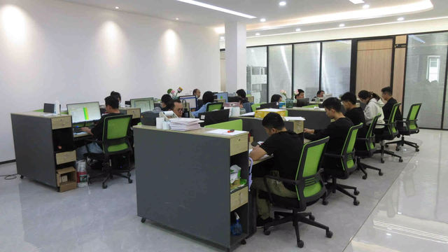
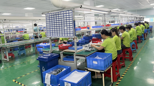
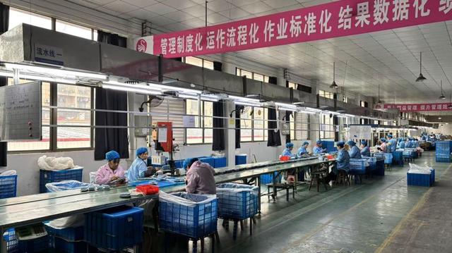
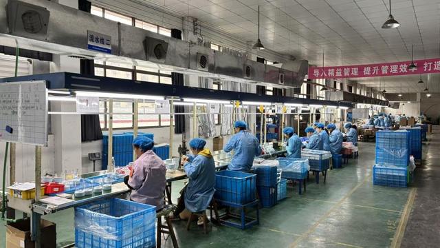
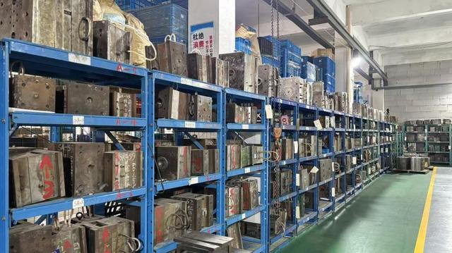
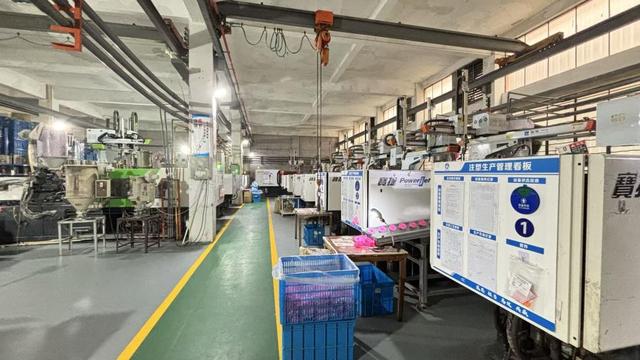
To ensure high standards of craftsmanship and reliability across all production runs, Chengdu Osity Beauty Co., Ltd. operates state-of-the-art production environments. This includes ISO 9001 and ISO 13485 compliant assembly floors, dedicated optical alignment labs, high-frequency circuit testing benches, and cleanroom facilities for medical-grade silicone molding.
Our collaborative setup bridges global logistics hubs with local engineering oversight, providing international clients with seamless tracking, quality verification reports, and expedited customs clearances. Explore our manufacturing, validation, and design workflows below: